




High-Resolution Imaging of Two-Dimensional Nanostructures
Mapping Quasi-Fermi Level Splitting, Perovskite Emission, and Exciton Dynamics
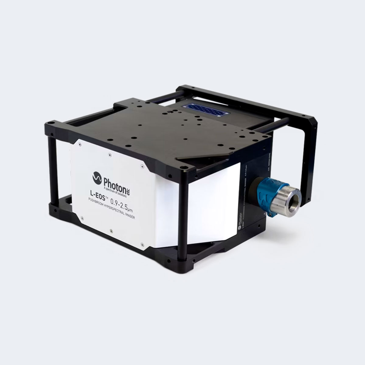
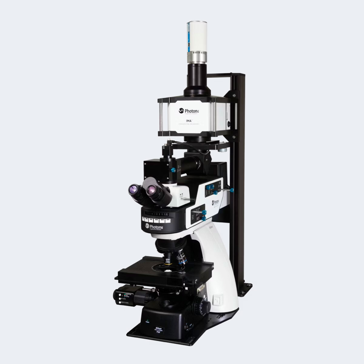
The rigorous characterization of 2D materials, such as MoS2, graphene, functionalized thin-film coatings, requires highly sensitive spatial and spectral characterization to fully understand their complex optoelectronic properties. Photon etc.’s IMA™ and Grand-EOS™ platforms deliver unparalleled high-resolution scalability for both small- and large-area hyperspectral and infrared imaging.
Powered by ultra-low-noise infrared cameras like the ZephIR™ and Alizé™ series and by our signature Volume-Bragg technology like the LLTF Contrast Laser Line Tunable Filter, Photon’s products enable researchers to rapidly extract and map critical electrical parameters in a matter of minutes.
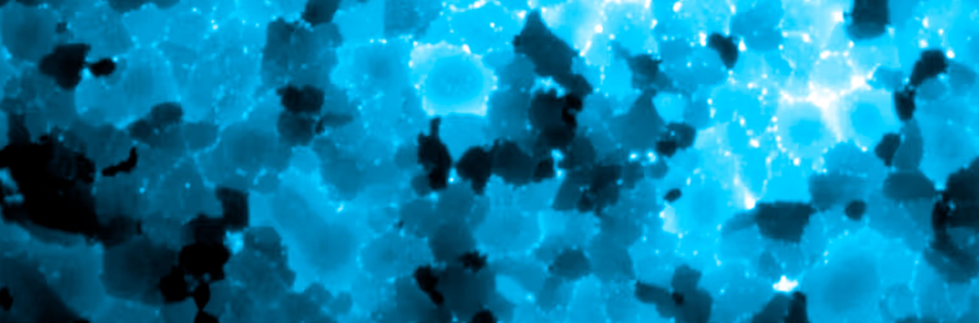
Such capabilities are essential for advanced 2D materials research where understanding nanoscale chemical heterogeneity and localized nanodomain growth is critical to evaluating material stability and performance. Whether analyzing monolayer MoS2 interfaces for photodetection, manipulating color emission in hybrid perovskites, or probing dark magnetic excitons in 2D multiferroics like NiI2, Photon has a product for every stage of the experimental journey.
Application domain
Related products

Fig. 1 – Source Wiley Advanced Online Library
For more information, contact info@photonetc.com

