






CIGS Spectral and Spatial Analysis
Renewable energy is gaining in popularity and the solar industry is taking off. This source of clean energy has the capacity to power the world and is growing at an exceptional rate. CIGS solar cells are excellent candidates for low-cost thin films-based panels and have shown impressive improvement in efficiency, now reaching more than 20% [1].
Application domain
Related products
Characterization of Losses in Patterning Grooves in CIGS Modules
One key feature that enables such high efficiency is the laser patterning interconnection that divides modules sized CIGS into smaller cells connected in series. However, even if this process helps the overall efficiency, it also incurs losses. This is why researchers are trying to find different patterning geometries.
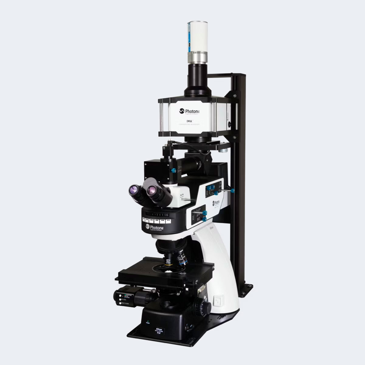
In this work [2] from Nice Solar, they focus on the damages caused by the laser ablation of two standard patterning grooves, P1 (patterning the back-contact) and P2 (used in the series interconnect). Damages are analysed by means of hyperspectral photoluminescence imaging. Photon etc.’s global hyperspectral platform (IMA) consists of an optical microscope coupled with a CW 532 nm laser and a hyperspectral filter based on volume Bragg gratings. This platform is sensitive from 400 nm to 1000 nm and provides both high spectral (<2 nm) and spatial resolution (~µm). Typical PL studies of CIGS are performed with localized excitation which leads to charge diffusion towards darker regions. The iso-potential created with global illumination reduces this effect and allows measurements to be performed closer to realistic operating mode of solar cells.

Fig. 1 – Observation anormale de PL aux abords de la ligne P1. a) Image optique des lignes d’ablation P1 et P2 (en haut) avec une carte d’intensité de PL extraite des données hyperspectrales capturées sur la même région (en bas); b) image de PL monochromatique (à 980 nm) des lignes de motifs P1 et P2 (en haut) avec analyse statistique des profils de PL (à 980 nm) à travers P1 et P2. (Seuls les profils représentatifs sont affichés; la moyenne a été effectuée sur l’ensemble des 25 profils.) Adaptée de [2].
The figure 1 shows the PL profile around P1 and P2 lines extracted from the hyperspectral data. The PL maps show a quenching of the emission near the edges of the P1 line. Further investigation showed that this effect accounts for ~30% reduction of the PL intensity, and is not due to compositional change. “This observation is unprecedented, and brings new insights for interconnection designs that are free of parasitic electrical paths induced by the P1 patterning line.” This work shows how hyperspectral imaging is a useful tool to identify losses and improve the efficiency of CIGS modules.

Study of Inhomogeneities in CIGS microcells
Another barrier to reaching higher efficiency in CIGS solar cells can be in part attributed to the cells inhomogeneity coming from its polycrystalline nature. To quantify the impact of the morphology on cell efficiency, studying the spatial variations of its different properties is paramount.
With this in mind, researchers at IPVF (formerly IRDEP – Institute of Research and Development on Photovoltaic Energy) investigated a CIGS microcell (diameter of 35 μm) through spectrally and spatially resolved photoluminescence (PL) and electroluminescence (EL) imaging [3]. To carry out such experiments they used an hyperspectral imager (IMA) with a 2 nm spectral resolution and a spatial resolution near the diffraction limit (~μm). A sourcemeter was employed for EL with Vapp = 0.95 V. A 532 nm laser was used for PL (excitation at 580 suns). The entire field of view under the microscope objective was excited and the PL signal coming from a million points was collected simultaneously.
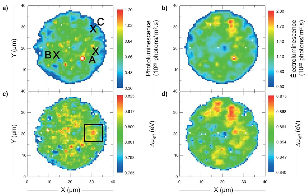
Fig. 2 – Hyperspectral images of a) integrated PL emission and b) integrated EL emission. Using the generalized Planck’s law, it is possible to deduce c) and d) Δμeff maps. Adapted from [3].
The figure 2 a) and b) present PL and EL images of the CIGS microcell. By combining their spectrally resolved PL and EL maps and a photometric absolute calibration method, researchers can use the generalized Planck’s law to extract the quasi-Fermi level splitting (Δμeff) (see Fig. 1 c) and d)) which is directly related to the maximum voltage of the cell. With the help of the reciprocity relation between solar cells and LEDs, the external quantum efficiency (EQE) can be deduced from the EL images.
Getting access to fundamental properties on a micrometer scale over the entire surface of the sample can help improve the fabrication process to reach higher cell efficiency.
[1] Yoshida S. et al. 2019, Solar frontier achieves world record thin-film solar cell efficiency of 23.35%. PR Team, Corporate Administration Department, Solar Frontier, 17 January 2019, accessed August 27th 2020.
[2] Quiroz, C. O. R., Dion-Bertrand, L.-I., Brabec, C. J., Müller, J., & Orgassa, K. (2020). Deciphering the origins of P1-induced power losses in CIGS modules through hyperspectral luminescence.
[3] Delamarre, A., Paire, M., Guillemoles, J.-F., & Lombez, L. (2014). Quantitative luminescence mapping of Cu(In, Ga)Se2 thin-film solar cells. Progress in Photovoltaics: Research and Applications, 23(10), 1305–1312.
For more information, contact info@photonetc.com
