




Nanophotonic Characterization of Metamaterials and Metasurfaces
Broadband Phase Profiling, Dispersion Engineering, and Analog Optical Computing
Metamaterials and metasurfaces are revolutionizing nanophotonics by enabling complex wavefront shaping, extreme polarization control, and advanced optoelectronics. To thoroughly characterize the unique optical properties of these sub-wavelength structures, researchers require precise, broadband spectral analysis tools. Enters the LLTF: featuring a continuous tuning range from 400 to 2500 nm and superior OD6 filtering, it delivers the highly selective illumination necessary to map diffraction efficiency and spatial phase profiles. Whether you are developing ultrathin silicon metagratings, superlenses, or vortex beam generators, Photon etc. provides the broadband analysis tools you need to accelerate your research.
Optical metasurfaces can also be designed to perform analog image processing such as spatial differentiation and edge detection. These metasurfaces hold the potential to reduce processing times and power consumption, while avoiding bulky 4 f lens systems. However, current designs have been suffering from trade-offs between spatial resolution, throughput, polarization asymmetry, operational bandwidth, and isotropy. Dispersion engineering provides an elegant way to design metasurfaces where all these critical metrics are simultaneously optimized. Silicon metasurfaces can perform isotropic and dual-polarization edge detection. Thanks to the low loss nature and dual-polarization response, these metasurfaces feature large throughput efficiencies, approaching the theoretical maximum for a given NA. OThese results pave the way for low-loss, high-efficiency and broadband optical computing and image processing with free-space metasurfaces.
Application domain
Related products
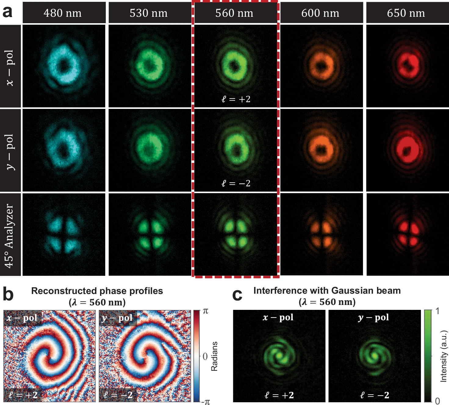
Fig. 1 – Source Nature Communications
Vortex beam generation by the bilayer metasurface: experiment results
a Intensity profiles of the orbital angular momentum (OAM) beams generated by the bilayer metasurface for different wavelengths. The first row shows the OAM mode with a topological charge of $\ell = +2$ when the incident polarization is along the $x$-axis. The second row represents the OAM mode with a topological charge of $\ell = -2$ for $y$-axis polarization. The third row shows the resulting petal-like interference patterns when a $45^\circ$ analyzer is introduced between the beam splitter and the camera, causing the $x$ and $y$ components to interfere, demonstrating the characteristic petal structure indicative of the interference of OAM modes with opposite topological charges. The red dotted box marks the output response at the design wavelength. b Reconstructed phase profiles of the generated OAM for the $x$- and $y$-polarization. c Measured spiral patterns created by the interference of the vortex beam and a co-propagating Gaussian beam. Depending on the sign of the topological charge $\ell = \pm2$, the helicity of the spiral is clockwise or counter-clockwise, respectively.
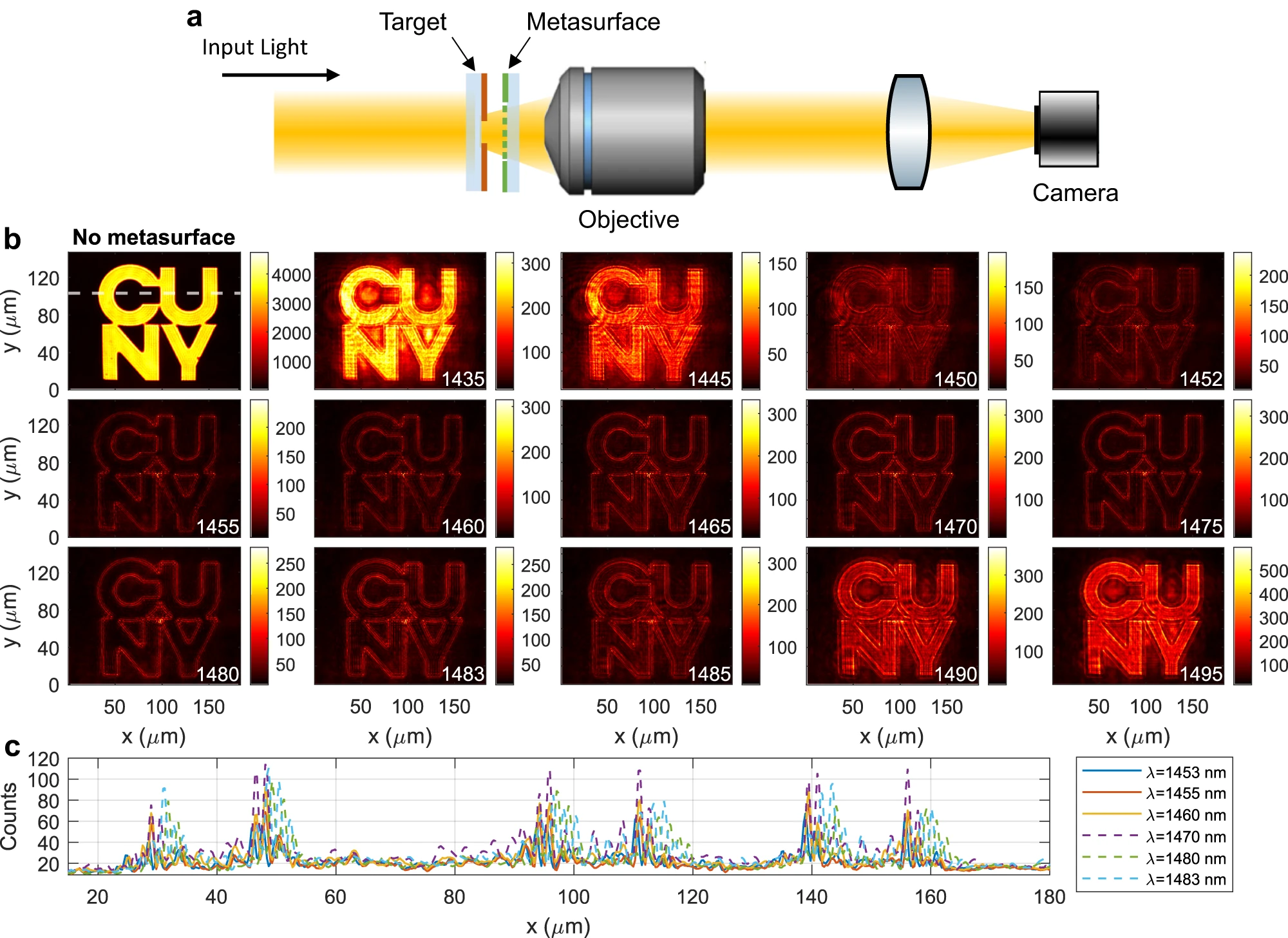
Fig. 2 – Source Nature Communications
Experimental edge detection with unpolarized narrow-band input
a Schematic of the setup used for the imaging experiments. b Top-left plot: Unfiltered image, obtained by removing the metasurface from the setup in panel a. All other colorplots show the output images obtained when the metasurface is placed in front of the target, for different impinging wavelengths (reported at the bottom-right corner of each plot). c Horizontal cuts of selected wavelengths from panel b (as indicated in the legend), corresponding to the vertical position denoted by the white dashed line in the top-left plot of panel b. For all measurements (with and without metasurface), the counts recorded by the camera have been normalized by the camera integration time and the power impinging on the target. The illumination is almost unpolarized (measured degree of polarization ≈ 10%).
For more information, contact info@photonetc.com
