





“The Dream Microscope” for Perovskite Research:
Unlocking the Secrets of Perovskite Solar Cells with Correlative Multimodal Microscopy
Application domain
Related products
About the Customer
Weber Microscopy Group | University of Stuttgart
Led by Professor Stefan Weber at the Institute for Photovoltaics of University of Stuttgart, the Weber Microscopy Group is an interdisciplinary team of researchers united by a shared passion for microscopy. Their mission: to bridge the gap between fundamental physics and functional photovoltaic devices by optimizing their underlying mechanics at the nanoscale.
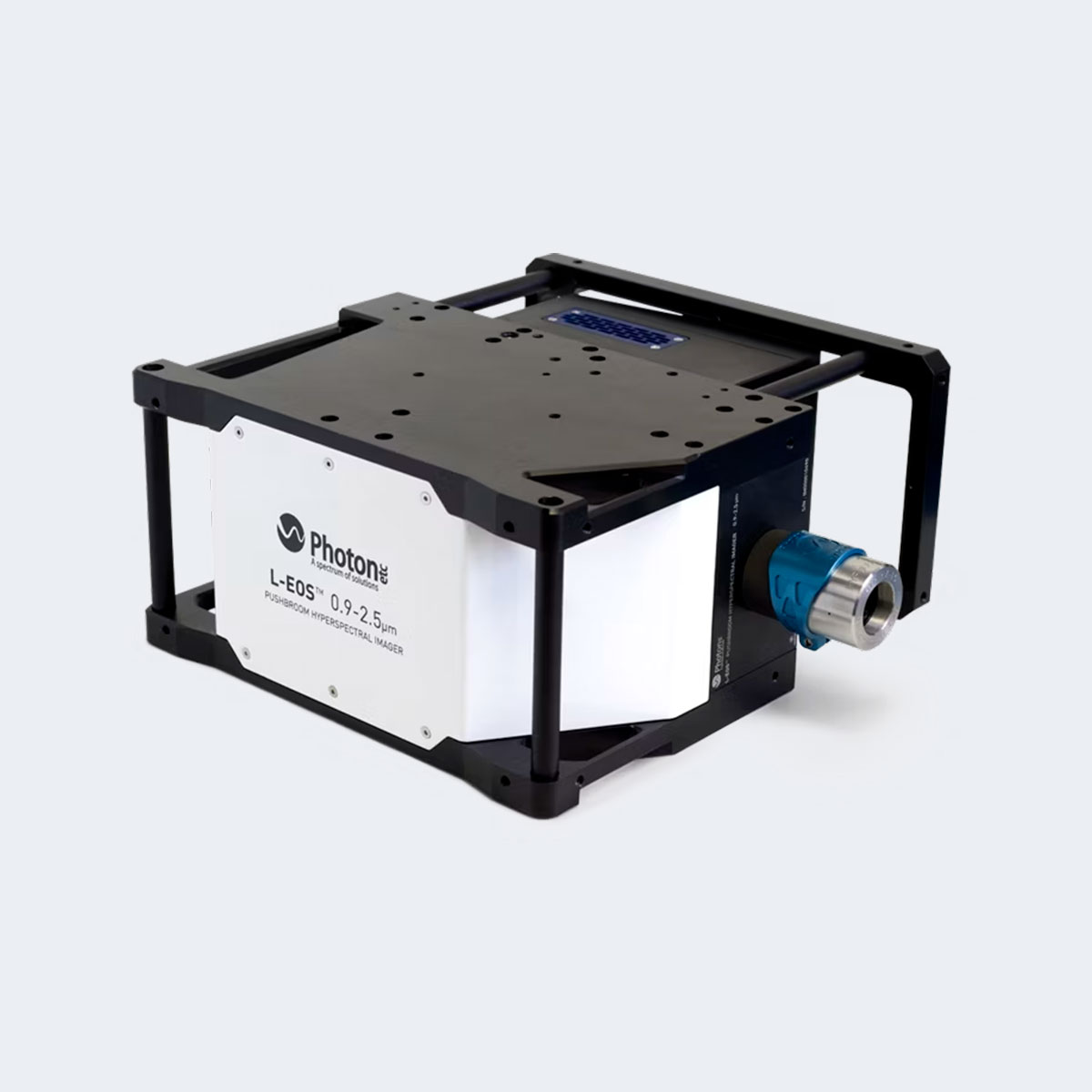
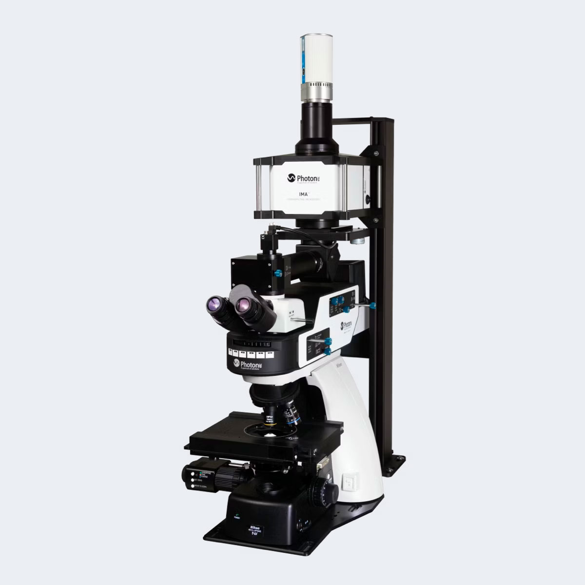
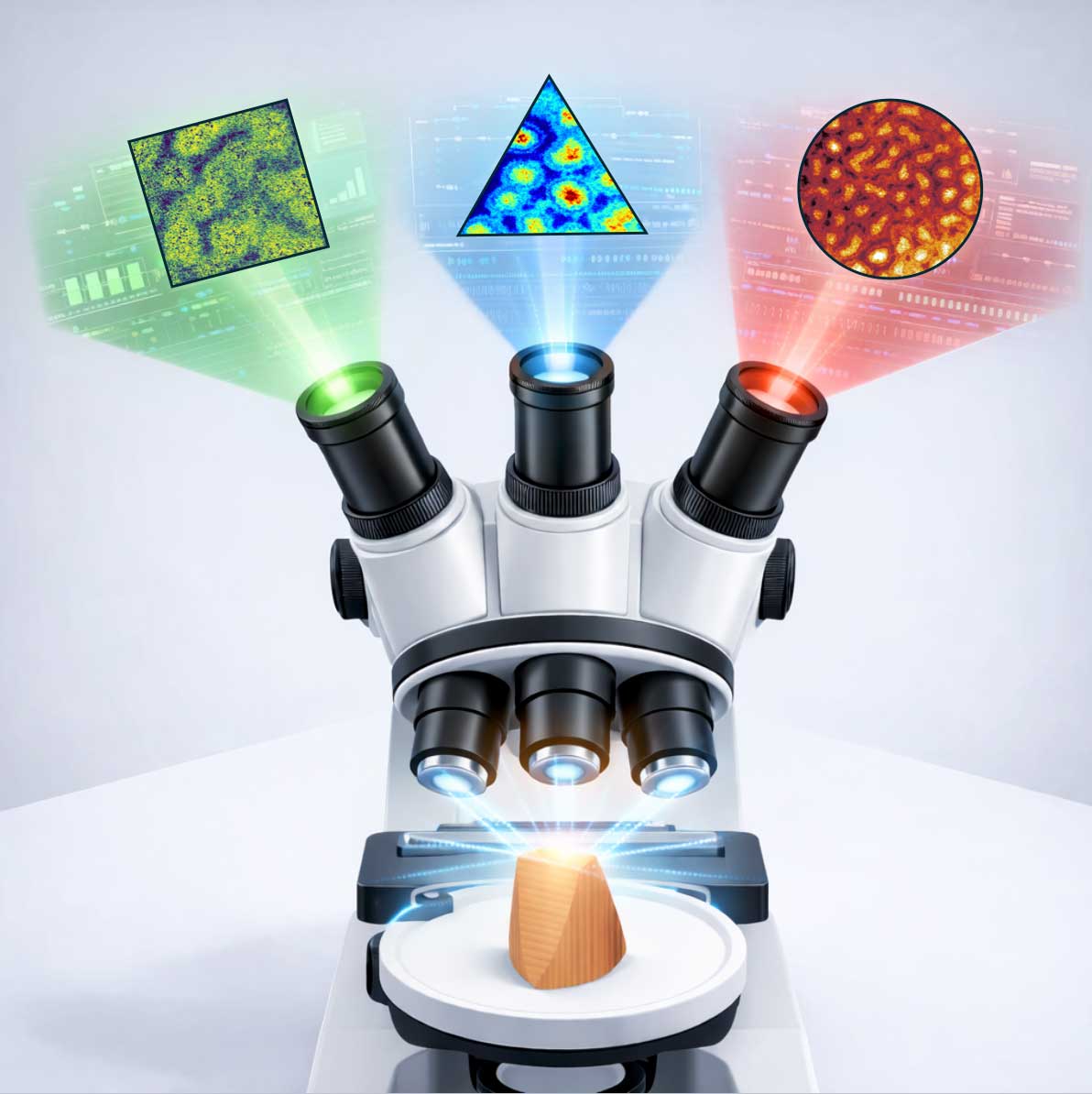
The group’s current focus is on one of the most promising and complex materials in novel photovoltaics, metal halide perovskite solar cells. Through their ERCfunded NanoPLoT project, Prof. Weber’s team has commissioned an innovative correlative microscopy platform that integrates Time-Resolved Photoluminescence Microscopy, Hyperspectral Imaging, and Atomic Force Microscopy (AFM).
This approach allows the team to directly associate structural defects to optoelectronic losses, revealing how crystalline anomalies influence a solar cell’s efficiency and long-term stability. This capability enables rapid defect identification, phase segregation analysis, and degradation tracking. This multimode system will undoubtedly prove a core tool in the group’s effort to unlocking stable, high-efficiency perovskite solar cells.
Technical Challenge
Linking Structure, Chemisty, and Carrier Dynamics
Developing the next generation of perovskite solar cells demands more than incremental improvements of individual characterization techniques, it requires tackling a fundamentally multidimensional problem.
No single microscopy modality can simultaneously probe the structural defects, chemical heterogeneities, mechanical strain, and carrier dynamics that collectively limit perovskite device performance and long-term stability. To understand how each variable affects the other, it is necessary to examine the problem from multiple sides. Only then will it be possible to elucidate its true nature and to tackle important physical questions that stand in the way of engineering tomorrow’s commercially-viable large-area panels.

The Solution: The “Dream Microscope”:
A Correlative Multimodal Platform For Perovskite Testing
Choosing the right testing equipment is a crucial part of the research process. The dream system must offer the high resolution needed to resolve intricate perovskite nanostructures, while also being versatile, reliable, and maintain a non-intrusive measurement profile. The instrument should adapt to the research, not the other way around.
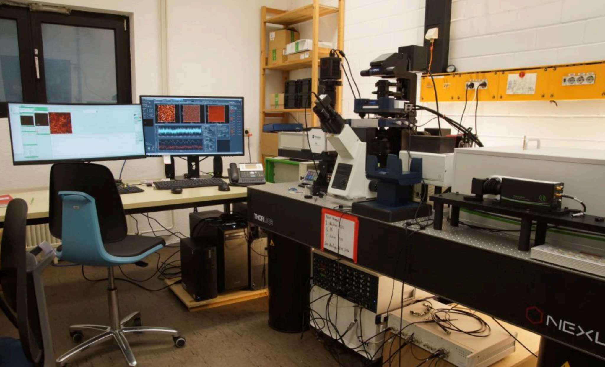
Seeking to contribute a new perspective to the perovskite field, Prof. Weber set out to design his ideal test system and backed by a generous ERC grant, he was able to bring the “Dream Microscope” into reality.
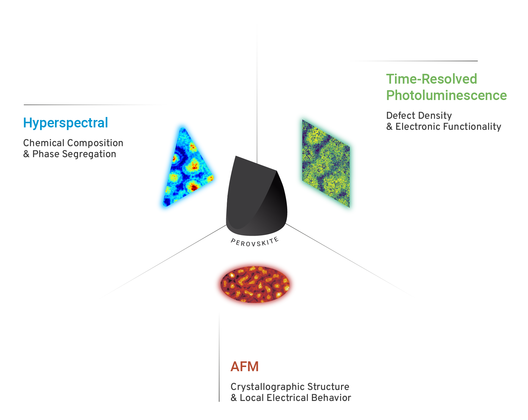
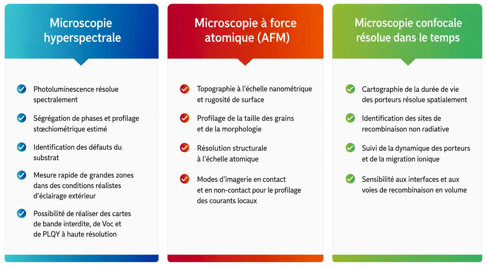
Key Insights From Three Microscopy Techniques
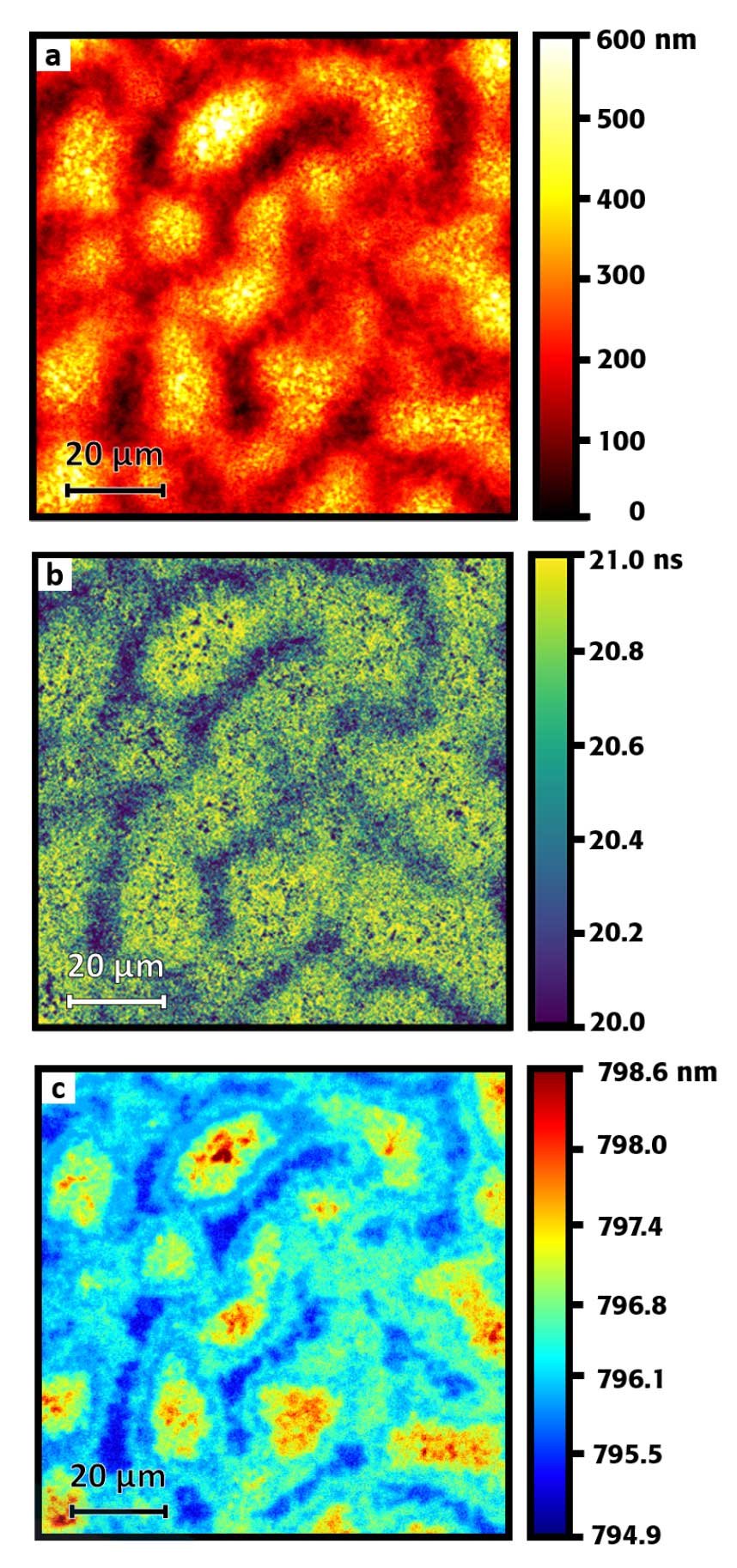
Results Preview I
Multimode characterization of a perovskite photovoltaic cell. (a) AFM micrograph showing a rugged topography. (b) Corresponding TRPL map showing high correlation between carrier lifetime to topography. (c) Corresponding hyperspectral spectrum peak mapping showing regions of phase segregation.
Scientific Advantage: NanoPLot’s Dream Microscope Technical Edge
Direct Connections Between Structure and Functionality Using Multimodal Microscopy
Although the system was just recently commissioned, Prof. Weber’s team is already “seeing” the difference of correlated measurements.
By injecting a local current with the AFM tip and measuring the corresponding tip-induced electroluminescence, the team is able to extract insights on carrier diffusion and lateral coupling between perovskite grains and optical waveguiding effects. The combination of spectroscopy and microscopy methods will enable unique characterization approaches for localized timeresolved experiments.
The correlation of AFM and time-resolved micrographs allows for the estimation of defect densities and reveals how variations in film thickness impact carrier lifetime and transport dynamics.
By comparing hyperspectral and AFM mappings, the team is able to relate film morphology to chemical composition throughout the substrate. Moreover, the correlation of time-resolved photoluminescence to hyperspectral mappings, reveals how phase segregation translates into electrical performance degradation over time.
The multimode approach provides a robust way to confirm or challenge assumptions about perovskite dynamics, and is a powerful compass to inform how variations in processing parameters impact improved stability and efficiency.
Before, research was limited by fragmented datasets, the lack of simultaneous compositional and morphological information, and long acquisition times that hindered targeted optimization.
These limitations created a gap in the identification of microscopic anomalies and limited the ability to associate them to macroscopic device performance. But now, the Dream Microscope has filled the void. The team can now draw direct connections between structure, chemistry, and function!
AFM gives me structural information and local electrical performance but it’s only part of the story… the other part of the story is told by the optical properties and the dynamics of photoluminescence. To get the full picture, we needed a combination of techniques — and that was basically the starting point. I asked myself, what would my dream microscope look like?
Dr Stefan Weber
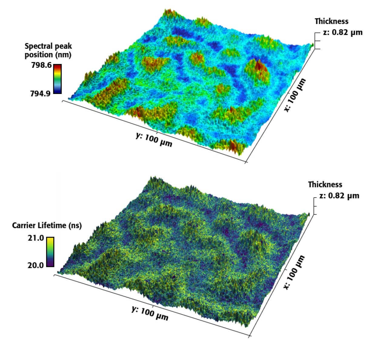
Results Preview II
Correlative microscopy of a perovskite solar cell surface. (Top) 3D overlay of AFM and Hyperspectral map showing that regions with larger thickness coincide with a higher spectral peak. (Bottom) 3D Overlay of AFM topography and Time-resolved photoluminescence showing that thinner regions in the perovskite valleys correlate with shorter carrier lifetimes.
Results Preview III
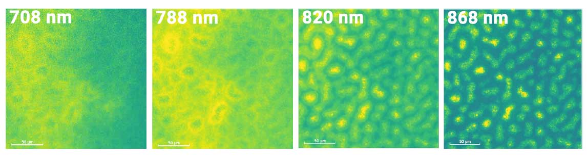
Hyperspectral photoluminescence maps showing spatial phase segregation and compositional heterogeneity in a perovskite thin film at four distinct emission wavelengths. Scale bars: 50 μm.
Results Preview IV
Correlative multi-modal microscopy transitions across a single field of view of a perovskite thin film. Each row demonstrates a progressive transition of co-localized images corresponding to AFM topography, TRPL lifetime mapping, and Hyperspectral imaging. The transitions highlight how localized perovskite grain morphology and domain boundaries directly dictate carrier lifetime dynamics and spectral emission features. Scale bars: 20 μm.
So far we have only scratched the surface of what’s possible with this microscope… you can really appreciate it in our group meetings, we are discussing for hours what we can see. It’s something really exciting, this system is a beast!
Prof. Stefan Weber

Future Outlook: Toward Durable Perovskites and Beyond!
Although current focus is on perovskite research, the Weber team already sees other research areas that could benefit from this correlative microscopy approach and they are looking forward to expanding into other research areas like:
- Semiconductor device inspection
- LED materials analysis
- Quantum dot characterization
- Advanced materials R&D
- Organic Solar Cell (OPV) improvement
The possibilities are endless and the science is no longer limited by the perspective of the instrument!
- Institute for Photovoltaics – University of Stuttgart
Prof. Dr. Stefan Weber Group Leader Nanoscale Microscopy and Characterization - PicoQuant- MicroTime 200
Picoquant Time-Resolved Photoluminescence Solutions - Photon Etc Hyperspectral Filter
- Bruker- Module AFM NanoWizard
For more information, contact info@photonetc.com
