






Organic Transistor Characterization
Quantifying Localized Energy Landscapes and Structural Uniformity in Semiconducting Macromolecules
The technological evolution of high-efficiency organic circuitry depends heavily on overcoming erratic charge transport mechanisms. Traditional carbon-based semiconducting thin films frequently suffer from profound spatial variations in molecular alignment and energy-level distribution, which trigger severe charge-trapping phenomena. These localized inconsistencies distort device metrics away from theoretical performance baselines, presenting a major barrier for engineering teams attempting to construct highly reproducible microelectronic systems with predictable switching behaviors.
To establish true performance consistency across active channel regions, contemporary electronic material research focuses on developing rigid, planar molecular architectures. By minimizing internal molecular flexing and promoting highly ordered structural stacking, these advanced polymer matrices create exceptionally smooth, uniform energetic pathways. The resulting electronic uniformity prevents the charge-carrier velocity from fluctuating under varying operating voltages, ensuring that the finished components maintain rock-solid reliability and operational longevity in ambient environments.
Uncovering the sub-micron variations that dictate these macroscopic electrical properties requires non-invasive optical profiling with exceptional spatial and spectral sensitivity. Wide-field photoluminescence mapping serves as a critical diagnostic technique in this regime, allowing engineers to track minute spectral shifts across mesoscopic scales. This optical methodology isolates highly ordered, high-performance domains from chaotic boundaries and structural anomalies, effectively linking local physical architecture directly to macroscopic device efficiency.
Application domain
Related products

IMA™ Platform
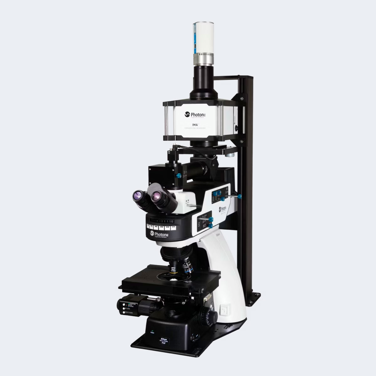
Photon etc.’s IMA™ wide-field hyperspectral imaging system was instrumental in directly mapping the nanoscale photoluminescence heterogeneity of the target polymer films. Utilizing an excitation wavelength of 405 nm and a low-noise silicon CCD detector, the platform recorded localized emission data across a vast spectrum from 600 to 1000 nm at a spatial resolution of 66 nm per pixel. This precise spectral discrimination allowed researchers to extract and calculate center-of-mass variations for 10,000 discrete points simultaneously, providing the definitive spatial data required to confirm a remarkably uniform energetic landscape across the transistor channel.
Source: Science Advances
Achieving ideal transistor characteristics in conjugated polymer semiconductors
For more information, contact info@photonetc.com
