







Advanced Optical Inspection Systems for Wide-Bandgap Semiconductors
Identifying Localized Crystal Defects and Physical Breakdown Mechanisms

GaN is rapidly establishing itself as a premier wide-bandgap semiconductor for next-generation high-power, high-frequency electronics. Its exceptionally high critical electric field and electron saturation velocity make it an attractive option in the fabrication of more energy-efficient and miniaturized devices. However, realizing the full performance potential of these devices demands a detailed understanding of how crystal defects, edge termination geometry, and radiation-induced damage affect local electric field distributions and recombination behavior.
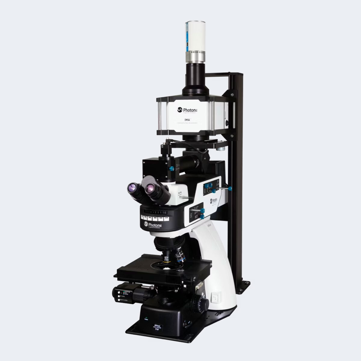
Photon etc.’s hyperspectral mapping technology provides Gallium Nitride (GaN) researchers with a sophisticated, non-destructive diagnostic tool that far exceeds the capabilities of conventional single-wavelength EL imaging. By capturing the unique spectral fingerprints of wide-bandgap materials across the UV-to-visible range, the IMA™ platform enables the precise identification and classification of diverse defect populations, including hot-electron sites and dislocations in PiN diodes. This spatial and spectral clarity allows scientists to pinpoint exact breakdown locations under high-voltage stress and evaluate how physical design alterations, like variations in anode thickness, influence overall device stability.
From initial device screening to long-term degradation and radiation hardness assessments, Photon etc. empowers researchers to visualize the complex physical properties of GaN devices with unparalleled detail.