Global Hyperspectral Imaging for the Next Generation of Advanced Materials
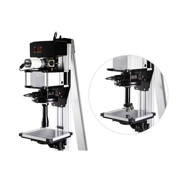
Conduct your optical measurements without damaging your film or device
An advanced material can be described as a new or transformed material that benefits from significant gains in efficiency compared to more traditional materials.
By using state-of-the-art photonics technology to capture high-resolution spectral data, hyperspectral imaging can provide a comprehensive understanding of the composition and properties of advanced materials. This information is critical for improving the performance and durability of these materials, making them more useful and effective for industrial applications. At Photon etc., we are leveraging the power of hyperspectral imaging to help shape the future of advanced materials technology.
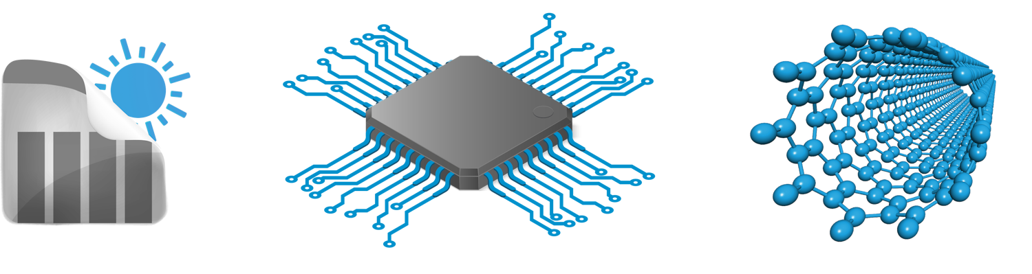
Photon etc. currently specialises in three key subsectors of advanced materials:
Solar materials Nanomaterials Semiconductors
Solar: Upscaling the development of new photovoltaic materials
The field of photovoltaic materials keeps expanding, and the variety of solar cells has never been so broad. Silicon is no longer the only candidate in the growing solar energy market: thin-film solar cells based on cadmium telluride (CdTe) or copper indium gallium selenium (CIGS) are taking their market share. In addition, perovskite is also gaining in popularity due to its high absorption efficiency and low-cost production. However, these new candidates require more advanced monitoring due to their more complex structure.
Hyperspectral imaging is a non-destructive technique that allows identification of defects, grain boundaries, phase segregation, mapping of inhomogeneities, quantifying deficient areas and understanding degradation processes. Hence, this technique allows to improve fabrication methods of those next generation of solar materials.
Nanomaterials: an array of potential applications
Nanomaterials, including plasmonic nanoparticles (such as gold, silver, copper) and carbon nanotubes, have a wide range of potential applications in fields such as medicine, electronics, photovoltaic cells, catalysis, and more. Photonic technology has an increasingly important role to play in the growth and advancement of these materials by allowing for precise control over their synthesis and manipulation.
Photonics offers the ability to control the size, shape, and surface chemistry of nanomaterials, which can greatly influence their physical and chemical properties. Additionally, hyperspectral imaging can be used to characterize and optimize nanomaterial properties, leading to more efficient and effective applications in these various fields.
Webinar : A Novel Global Hyperspectral Darkfield Imaging Technique
Semiconductors: enhanced performance checks with hyperspectral imaging
Semiconductors are a crucial element of electronic devices such as computers, smartphones, tablets, medical equipment and gaming consoles. With the increasing demand for smaller and more powerful devices, the semiconductor industry is constantly looking for ways to improve their performance. Spectroscopic tools have the potential to enhance the growth of semiconductors by enabling faster and more accurate testing, allowing for better quality control during manufacturing processes, and developing new materials and processes that can improve the performance of semiconductors.
Global Imaging
Global hyperspectral imaging is a non-destructive technique combining spectroscopy and imaging; where each image is acquired at a narrow band of wavelength. Spectrally and spatially resolved photoluminescence, electroluminescence, transmittance and reflectance data can be acquired. When analyzing this combination of spatial and spectral information, it is possible to tag certain spectral signatures and attribute them to elements of a given sample.In contrast, a spectral measurement performed with a line-scan or point-by-point technology requires the sample, the sensor, or the excitation source to move. Global imaging does not require image reconstruction and also, since the whole field of view is imaged simultaneously, moving object trajectories can be reconstructed.
In most confocal setups, the excitation is done in one point (~1μm2) which leaves the surrounding area at rest. This leads to lateral diffusion of charges towards darker regions. This has the effect of reducing the PL signal intensity. So the excitation power needs to be increased considerably in order to observe the signal. Also, this high-power density is far from what the PV material will experience in real conditions. Whereas in global imaging, the uniform illumination reduces the charge diffusion. This uniform illumination allows carrying PL experiments in the range of 0.1 suns or up to 500 suns which is within the range of realistic operating mode of PV material.
Our Products

IMA™
IMA is a hyperspectral microscope delivering spectral and spatial information in the VIS, NIR and/or SWIR spectral ranges (400 nm - 1620 nm).
GRAND-EOS™
GRAND-EOS is a global hyperspectral camera continuously tunable from 400 nm to 1650 nm. This system combines micro and macro modalities.

LLTF CONTRAST™
The LLTF CONTRAST is a non-dispersive tunable (400-2500 nm) bandpass filter based on volume Bragg gratings.

V-EOS™
V-EOS is a global hyperspectral camera continuously tunable from 400 to 1000 nm.

S-EOS™
S-EOS is a global hyperspectral camera continuously tunable from 900 to 1620 nm or from 900 to 2500 nm.