

Leverage the Power of Hyperspectral Microscopy
IMA is a hyperspectral microscope delivering spectral and spatial information from 400 nm to 1620 nm in one single instrument. By combining a scientific grade VIS, NIR, and/or SWIR microscope with Photon etc patented imaging filter, extensive optical characterization can be achieved on a wide variety of materials. Our hyperspectral imaging microscope is capable of acquiring millions of data points in a single snapshot and rapidly maps photoluminescence (PL), electroluminescence (EL), fluorescence, reflectance, and transmittance. IMA offers the flexibility to be configured as either a brightfield or a darkfield hyperspectral microscope. Moreover, based on high throughput imaging filters, IMA is a faster and more efficient hyperspectral imaging system than standard point-by-point scanning systems.
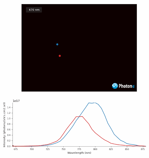
PL monochromatic images of Perovskite crystals excited at the equivalent power of 10 suns with spectra from regions of Perovskite crystals designated by the blue and red targets.
IMA Applications Overview
- Perform complex material analyses such as solar cell characterization, nanomaterials, and semiconductor quality control by means of hyperspectral microscopy (PL, EL).
- Study novel IR markers in complex environments including live cells and tissue through Photon etc’s hyperspectral SWIR microscope.
- Take advantage of a darkfield hyperspectral microscope to reveal nanoparticle properties on transparent, unstained samples, such as polymers, crystals, and living cells.
Welcome the future of hyperspectral microscopy with IMA – a precise and efficient partner in your exciting scientific journey.
Product Specifications
| VIS | SWIR | |
|---|---|---|
| Spectral range | 400-1000 nm | 900-1620 nm |
| Spectral resolution (FWHM) | < 2 nm | < 4 nm |
| Spectral channels | Continuously tunable | Continuously tunable |
| Spatial resolution | Sub-micron - limited by the microscope objective NA | Sub-micron - limited by the microscope objective NA |
| Camera | CCD, EMCCD, sCMOS | Photon etc. InGaAs camera (ZephIR™ 1.7 or Alizé™ 1.7) |
| Excitation wavelengths (up to 3 lasers) | 405, 447, 532, 561, 660, 730, 785, 808 nm (other wavelenghts available upon request) | 405, 447, 532, 561, 660, 730, 785, 808 nm (other wavelenghts available upon request) |
| Microscope | Upright or inverted, scientific grade | Upright or inverted, scientific grade |
| White light illumination | Diascopic, episcopic, Hg, halogen | Diascopic, episcopic, Hg, halogen |
| Illumination options | Epifluorescence module, darkfield module (oil or dry) | Epifluorescence module, darkfield module (oil or dry) |
Spec Sheet
Publications
Nature
- Perovskite
Autonomous closed-loop framework for reproducible perovskite solar cells
Artificial Intelligence in the Life Sciences
- Fluorescence
Development of a deep neural network model for simultaneous analysis of extracellular analyte gradients for a population of cells
Advanced Optical Materials
- Perovskite
Boosting the Performance of Epitaxial Perovskite Microstructures by Surface Passivation
Royal Society of Chemistry
- Perovskite
Hole-transport layer-dependent degradation mechanisms in perovskite solar modules
Solar RRL
- Perovskite
Strategies for Quasi-2D Integration in Perovskite p-i-n Solar Cells
Advanced Materials
- Perovskite
Carrier Diffusion Links Single Crystal Quality and Photoluminescence in Halide Perovskite Radiation Detectors
Advanced Materials
- Perovskite
High Light Utilization and Color Rendering in Vacuum-Deposited Semitransparent Perovskite Solar Cells
Applied Energy Materials
- Perovskite
Temperature-Resilient Monolithic Perovskite/Silicon Tandems Enabling Crystalline Front TCO Integration
Journal of the American Chemical Society
- Perovskite
Crystal Growth Modulation of Tin–Lead Halide Perovskites via Chaotropic Agent
Computers in Biology and Medicine
- Oncology
A hyperspectral imaging dataset and Grassmann manifold method for intraoperative pixel-wise classification of metastatic colon cancer in the liver
Advanced Functional Materials
Photophysical and Viscoelastic Properties of Ionically Complexed Conjugated Polyelectrolyte for Printed Soft Electronics
Nature nanotechnology
- Perovskite
Dynamic nanodomains dictate macroscopic properties in lead halide perovskites
ACS Applied Materials & Interfaces
- Perovskite
In Situ Film Stress Measurements Capture Increased Photostability in Additive-Engineered Mixed-Halide Perovskites
Progress in Photovoltaics: Research and Applications
- Perovskite
- Si
Photostable Inorganic Perovskite Absorber via Thermal Evaporation for Monolithic Perovskite/Perovskite/Silicon Triple-Junction Solar Cells
Nano Micro Small
- Perovskite
Quasi-2D Scaffolding for Enhanced Stability and Efficiency in 1.67 eV Cs-Rich Pure-Iodide Perovskite Solar Cells
Nature Communications
- Perovskite
Local halide heterogeneity drives surface wrinkling in mixed-halide wide-bandgap perovskites
ACS Energy Letters
- Perovskite
Optimised graphene-oxide-based interconnecting layer in all-perovskite tandem solar cells
Journal of Materials Chemistry A
- Perovskite
Compositional and interfacial engineering for improved light stability of flexible wide-bandgap perovskite solar cells
Small Science
- Carbon Nanotubes
Programming-Assisted Imaging of Cellular Nitric Oxide Efflux Gradients and Directionality via Carbon Nanotube Sensors
Nature communications
- Perovskite
Solvent-dripping modulated 3D/2D heterostructures for high-performance perovskite solar cells
SpringerNature
- Perovskite
The role of TCNQ for surface and interface passivation in inverted perovskite solar cells
Joule
- Perovskite
- Si
Efficient blade-coated perovskite/silicon tandems via interface engineering
Nature Energy
- Perovskite
Diamine chelates for increased stability in mixed Sn–Pb and all-perovskite tandem solar cells
ACS Publications
- Oncology
Machine Learning-Assisted Near-Infrared Spectral Fingerprinting for Macrophage Phenotyping
Advanced Materials
- Perovskite
Nanometer Control of Ruddlesden-Popper Interlayers by Thermal Evaporation for Efficient Perovskite Photovoltaics
Nature Communications
- Perovskite
Strong angular and spectral narrowing of electroluminescence in an integrated Tamm-plasmon-driven halide perovskite LED
Nature communications
- Perovskite
Quantum barriers engineering toward radiative and stable perovskite photovoltaic devices
Advanced Functional Materials
- Perovskite
Squeezing the Threshold of Metal-Halide Perovskite Micro-Crystal Lasers Grown by Solution Epitaxy
Energy & Environmental Science
- Perovskite
Physics-based material parameters extraction from perovskite experiments via Bayesian optimization
ACS Energy Letters
- Perovskite
Electrochemical Impedance Spectroscopy of All-Perovskite Tandem Solar Cells.
nature
- Perovskite
Sublimed C60 for efficient and repeatable perovskite-based solar cells
AIP Publishing
- Graphene
Spectroscopic analysis of polymer and monolayer MoS2 interfaces for photodetection applications
Nature Machine Intelligence
- Perovskite
Self-supervised deep learning for tracking degradation of perovskite light-emitting diodes with multispectral imaging
Advanced Materials
- Perovskite
Fabrication of low-cost and flexible perovskite solar cells by slot-die coating for indoor applications
Advanced Functional Materials
- Perovskite
Direct Visualization of Chemically Resolved Multilayered Domains in Mixed-Linker Metal–Organic Frameworks
Nature Chemical Biology
- Oncology
Nanosensor-based monitoring of autophagy-associated lysosomal acidification in vivo
Science Advances
- Other Semiconductors
Achieving ideal transistor characteristics in conjugated polymer semiconductors
Cornell University
- Perovskite
Imaging Light-Induced Migration of Dislocations in Halide Perovskites with 3D Nanoscale Strain Mapping
ACS Chemical Biology
- Oncology
Hematoxylin Nuclear Stain Reports Oxidative Stress via Near-Infrared Emission
ACS Applied Energy Materials
- Perovskite
Identification and Mitigation of Transient Phenomena That Complicate the Characterization of Halide Perovskite Photodetectors
American Chemical Society Sensors
- Biochemistry & Nanosensors
Physicochemical Profiling of Macrophage Heterogeneity Using Deep Learning Integrated Nanosensor Cytometry
Nano, Micro, Small
- Nanoparticles
Learning and Predicting Photonic Responses of Plasmonic Nanoparticle Assemblies via Dual Variational Autoencoders
American Chemical Society
- Nanoparticles
Strongly Confined CsPbBr3 Quantum Dots as Quantum Emitters and Building Blocks for Rhombic Superlattices
Advanced Functional Materials
- Perovskite
Monolithic Perovskite/Silicon Tandems with >28% Efficiency: Role of Silicon-Surface Texture on Perovskite Properties
Australian PV Institute
- Si
Development of Inkjet-Printed Doping for Poly-Si Passivating Contacts in Silicon Solar Cells
Nanoscale Advances
- Nanoparticles
Direct 3D-printed CdSe quantum dots via scanning micropipette
ACS Publications
- Perovskite
Tunable Multiband Halide Perovskite Tandem Photodetectors with Switchable Response
Nature
- Perovskite
Regulating surface potential maximizes voltage in all-perovskite tandems
XLIII Jornadas de Automática
- Life Sciences
Digital staining of multispectral microscopic images. Application to breast cancer indentification
ACS Publications
- Perovskite
Ethylenediamine Addition Improves Performance and Suppresses Phase Instabilities in Mixed-Halide Perovskites
Advanced Materials
- Perovskite
Manipulating Color Emission in 2D Hybrid Perovskites by Fine Tuning Halide Segregation: A Transparent Green Emitter
Royal Society of Chemistry
- Perovskite
Taking a closer look – how the microstructure of Dion–Jacobson perovskites governs their photophysics
Advanced Functional Materials
- Perovskite
Shape-Controlled Solution-Epitaxial Perovskite Micro-Crystal Lasers Rivaling Vapor Deposited Ones
Advances Functional Materials
Charge Extraction in Flexible Perovskite Solar Cell Architectures for Indoor Applications – with up to 31% Efficiency
Nature communications
- Perovskite
Imaging and quantifying non-radiative losses at 23% efficient inverted perovskite solar cells interfaces
Advanced Optical Materials
- Perovskite
Highly Stable Lasing from Solution-Epitaxially Grown Formamidinium-Lead-Bromide Micro-Resonators
Frontiers in Pharmacology
- Pharmacology
Metabolic Consequences of Developmental Exposure to Polystyrene Nanoplastics, the Flame Retardant BDE-47 and Their Combination in Zebrafish
Optical Materials
- Perovskite
Understanding the impact of SrI2 additive on the properties of Sn-based halide perovskites
Nature Nanotechnology
- Perovskite
Nanoscale chemical heterogeneity dominates the optoelectronic response of alloyed perovskite solar cells
Energy Environmental Science
- Perovskite
Ligand-bridged charge extraction and enhanced quantum efficiency enable efficient n–i–p perovskite/silicon tandem solar cells
ACS Energy Letters
- Photovoltaics
Multimodal Microscale Imaging of Textured Perovskite−Silicon Tandem Solar Cells
Advanced Functional Materials
- Perovskite
Revealing Nanomechanical Domains and Their Transient Behavior in Mixed-Halide Perovskite Films
Nanomaterials
- Carbon Nanotubes
- Life Sciences
Quantification of Nitric Oxide Concentration Using Single-Walled Carbon Nanotube Sensors
Joule
- Photovoltaics
Rapid Open-Air Fabrication of Perovskite Solar Modules
Physical Chemistry Chemical Physics
- Photovoltaics
Unraveling Antisolvent Dripping Delay Effect on Stranski-Krastanov Growth of CH3NH3PbBr3 Thin Films: A Facile Route for Preparing Textured Morphology with Improved Optoelectronic Properties
Journal of Applied Physics
- Photovoltaics
Investigation of the spatial distribution of hot carriers in quantum-well structures via hyperspectral luminescence imaging
Nano Letters
- Life Sciences
Nanoreporter of an Enzymatic Suicide Inactivation Pathway
Journal of Applied Physics
- Photovoltaics
Intermediate scale bandgap fluctuations in ultrathin Cu(In,Ga)Se2 absorber layers
Advanced Functional Materials
- Photovoltaics
Epitaxial Metal Halide Perovskites by Inkjet‐Printing on Various Substrates
Engineering
- Photovoltaics
Deciphering the Origins of P1-Induced Power Losses in CIGS Modules Through Hyperspectral Luminescence
ACS Applied Materials Interfaces
- Photovoltaics
Cosolvent Effects When Blade-Coating a Low-Solubility Conjugated Polymer for Bulk Heterojunction Organic Photovoltaics
Joule
- Photovoltaics
Proton Radiation Hardness of Perovskite Tandem Photovoltaics
ACS Energy Letter
- Photovoltaics
Stable Hexylphosphonate-Capped Blue Emitting Quantum-Confined CsPbBr3 NanoPlatelets
The Journal of Physical Chemistry C
- Photovoltaics
Imaging Electron, Hole and Ion Transport in Halide Perovskite
ACS Energy Letters
- Photovoltaics
Visualizing and Suppressing Nonradiative Losses in High Open-Circuit Voltage n‑i-p-Type CsPbI3 Perovskite Solar Cells
Advanced Materials
- Photovoltaics
Controlling the Growth Kinetics and Optoelectronic Properties of 2D/3D Lead–Tin Perovskite Heterojunctions
Advanced Materials
- Photovoltaics
A Highly Emissive Surface Layer in Mixed-Halide Multication Perovskites
Advanced Functional Materials
- Photovoltaics
Interface Molecular Engineering for Laminated Monolithic Perovskite/Silicon Tandem Solar Cells with 80.4% Fill Factor
Nano Letters
- Carbon-Based Materials
- Life Sciences
Biomolecular Functionalization of a Nanomaterial To Control Stability and Retention within Live Cells
Semiconductor Science and Technology
- Photovoltaics
A Hot-Carrier Assisted InAs/AlGaAsQuantum-Dot Intermediate-Band Solar Cell
Nano Letters
- Carbon-Based Materials
- Biochemistry & Nanosensors
- Oncology
An in Vivo Nanosensor Measures Compartmental Doxorubicin Exposure
SPIE Medical Imaging: Digital Pathology
- Life Sciences
Hyperspectral Imaging for Intraoperative Diagnosis of Colon Cancer Metastasis in a Liver
Advanced Functional Materials
- Nanoparticles
Decoupling Theranostics with Rare Earth Doped Nanoparticles
ACS Nano
- Carbon-Based Materials
- Biochemistry & Nanosensors
- Oncology
A Carbon Nanotube Optical Reporter Maps Endolysosomal Lipid Flux
ACS Nano
- Carbon-Based Materials
- Life Sciences
A Carbon Nanotube Optical Sensor Reports Nuclear Entry via a Noncanonical Pathway
Nature Biomedical Engineering
- Carbon-Based Materials
- Biochemistry & Nanosensors
- Oncology
A Carbon Nanotube Reporter of MicroRNA Hybridization Events In Vivo
Analytical Chemistry
- Carbon-Based Materials
- Life Sciences
Single Nanotube Spectral Imaging To Determine Molar Concentrations of Isolated Carbon Nanotube Species
ECS Journal of Solid State Science and Technology
Hyperspectral Electroluminescence Characterization of OFF-State Device Characteristics in Proton Irradiated High Voltage AlGaN/GaN HEMTs
Applied Physics Letters
- Photovoltaics
On the Origin of the Spatial Inhomogeneity of Photoluminescence in Thin-Film CIGS Solar Devices
Energy & Environmental Science
- Photovoltaics
Quantification of Spatial Inhomogeneity in Perovskite Solar Cells by Hyperspectral Luminescence Imaging
Journal of Biomedical Optics
- Biochemistry & Nanosensors
- Neuroscience
Hyperspectral Multiplex Singleparticle Tracking of Different Receptor Subtypes Labeled with Quantum Dots in Live Neurons
Physical Review Applied
- Other Semiconductors
Optical Imaging of Light-Induced Thermopower in Semiconductors
Scientific Reports
- Carbon-Based Materials
- Biochemistry & Nanosensors
Hyperspectral Microscopy of Near Infrared Fluorescence Enables 17-Chirality Carbon Nanotube Imaging
Carbon
- Carbon-Based Materials
- Biochemistry & Nanosensors
- Oncology
Photoluminescent Carbon Nanotubes Interrogate the Permeability of Multicellular Tumor Spheroids
SPIE: Imaging, and Spectroscopy
- Nanoparticles
- Biochemistry & Nanosensors
Dark-Field Spectral Imaging Microscope for Localized Surface Plasmon Resonance-Based Biosensing
Nanoscale
- Life Sciences
Cellulose Nanocrystals With Tunable Surface Charge for Nanomedicine
SPIE: Imaging, Manipulation, and Analysis of Biomolecules, Cells, and Tissues XIII
- Biochemistry & Nanosensors
- Neuroscience
Hyperspectral imaging to monitor simultaneously multiple protein subtypes and live track their spatial dynamics: a new platform to screen drugs for CNS diseases
Progress in Photovoltaics: Research and Applications
- Photovoltaics
Quantitative Luminescence Mapping of Cu(In, Ga)Se2 Thin-Film Solar Cells
Sensors and Actuators B: Chemical
- Biochemistry & Nanosensors
GaAs/AlGaAs Heterostructure Based Photonic Biosensor for Rapid Detection of Escherichia Coli in Phosphate Buffered Saline Solution
Applied Surface Science
- Advanced materials
- Life Sciences
Solvent-Mediated Self-Assembly of Hexadecanethiol on GaAs (001)
Applied Physics Letters
- Advanced materials
Experimental Evidence for Mobile Luminescence Center Mobility on Partial Dislocations in 4h-Sic Using Hyperspectral Electroluminescence Imaging
SPIE: Physics, Simulation, and Photonic Engineering of Photovoltaic Devices II
- Photovoltaics
Evaluation of Micrometer Scale Lateral Fluctuations of Transport Properties in CIGS Solar Cells
Light: Science & Applications
- Advanced materials
- Life Sciences
Conic Hyperspectral Dispersion Mapping Applied to Semiconductor Plasmonics
Applied Physics Letters
- Photovoltaics
Contactless Mapping of Saturation Currents of Solar Cells by Photoluminescence
SPIE: Physics, Simulation, and Photonic Engineering of Photovoltaic Devices
- Photovoltaics
Characterization of Solar Cells Using Electroluminescence and Photoluminescence Hyperspectral Images
Sensors and Actuators B: Chemical
- Biochemistry & Nanosensors
A Photoluminescence-Based Quantum Semiconductor Biosensor for Rapid in Situ Detection of Escherichia Coli
Applied Surface Science
- Life Sciences
Molecular Self-Assembly and Passivation of GaAs (001) With Alkanethiol Monolayers: A View Towards Bio-Functionalization
Journal of Applied Physics
- Life Sciences
Formation Dynamics of Hexadecanethiol Self-Assembled Monolayers on (001) GaAs Observed With Photoluminescence and Fourier Transform Infrared Spectroscopies
Videos
Photovoltaic Analysis Made Simple : PLQY and QFLS Mapping in Minutes
With the rise of new photovoltaic materials, relying on PLQY mapping alone is no longer enough to evaluate performance. Using data acquired by IMA hyperspectral microscope, our new software module lets you generate essential photovoltaic characterization maps: PLQY, QFLS, and Eg in just a few clicks for deeper, more accurate insights.
Whether you’re just getting started or deep into materials optimization, this tool is fast, reliable, and ready to plug into your solar research workflow.
ASU Core Facilities Equipment Showcase: Photon etc. Hyperspectral Microscope
From mapping compositions to identifying defects, discover below how ASU Core Research Facilities are leveraging our IMA for their research in solar cell characterization, nanomaterials, and semiconductor.
Hyperspectral Characterization of Next-Generation Solar Cells and LEDs
This video shows how spectrally and spatially resolved PL and EL maps can help identify defects, losses, and uniformity in advanced materials. A hyperspectral photoluminescence demonstration is performed on large grain perovskite crystals.
Photon etc.’s Global Imaging Technology
This video shows the conceptual difference between hyperspectral global imaging and raster scan (line scan, pushbroom). With global imaging, only a few monochromatic images are required to obtain a hyperspectral cube of data (X-Y spatial, Z spectral). With raster scan technologies, a spectrum needs to be acquired on each point/line within the desired field of view.
IMA - Hyperspectral Microscope
From solar cells to live cell imaging, this global hyperspectral microscope, IMA, rapidly provides spectrally and spatially resolved maps in the VIS, NIR and SWIR ranges. Hyperspectral fluorescence, photoluminescence, electroluminescence, reflectance and transmittance measurements can be obtained. Darkfield and brightfield modalities are available.
Silicon Carbide Defect Characterization
This video shows how various types of defects in SiC can easily be detected using electroluminescence maps obtained with Photon etc’s hyperspectral imaging system, IMA. Offering spectrally resolved images, Photon etc’s hyperspectral imaging technology improves advanced material development capacities.